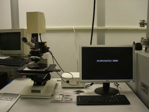
Nanospec 3000
- Computerized film thickness measurement system
- Computer controlled grating monochromator
- Photomultiplier tube detector
- Film thickness is calculated based on the interference spectra generated when the light passes thru the film using one of several proprietary algorithms
- Offers fast measurements and multilayer film capability
- Safety
- Burn Hazard: The light source is hot. Be careful when aligning the light bulb.
- Strong Light Hazard: Do not look into the light source directly for a long period of time.
- Statistical/Process Data
- Nanospec is tested by process staff monthly using standard wafer
- Available Processes, Gases, Process Notes
- Standard programs provided by the instrument vendor are listed
- In order to measure the film thickness, the refractive index and extinctive coefficient of the film are needed. The instrument vendor provided these data of various films, which are listed
- Nanospec can only measure transparent films. Metal films and thick Germanium/Silicon films cannot be measured.
- Contact process staff to set new measurement program if needed.
- System Description
- The Nanospec system consists of a customized optical microscope and a personal computer with Windows OS.
- The optical microscope has a computerized spectrophotometer head and a dual wafer stage, left side for the reference wafer and right side for the sample to be measured. The microscope has three objective lenses: 5X, 10X (default), and 50X magnifications. There are three tabs on the light path of the microscope. Their functions are described below.
- Field: Labeled with F. It can be rotated to change the size of the octagon in the field of view. The octagon is used for focusing when measuring blank sample without patterns and the reference wafers. It may be difficult to focus on all eight edges of the octagon. The user can just pick one edge for focusing. Then repeat on the same edge for consistent measurement results.
- Aperture: Labeled with A. It controls the light intensity and usually needs no adjusting.
- Filter: not labeled tab that moves left or right. It inserts a yellow color filter in the light path to prevent light exposure, when measuring photo-resist.
- All the system operations are controlled by clicking the GUI buttons showed on the personal computer screen. Most used GUI buttons are listed in the following sections.
- CALIB Stops any measurement in progress and returns to the available Program Screen. A new program is selected by double clicking on the program name. Before the selected program starts, the computer will prompt for a reference calibration sequence.
- ENTER Terminates an alphanumeric entry. The entry is not stored in the computer until this key is clicked.
- GRAPH Displays the measurement result in the graphic format.
- LIST Displays all the current measurement results in the numeric table format.
- MEAS Starts a measurement.
- NEW TEST Clears all the previous measured data from the screen. Starts a new numeric table and statistics for the new measurements.
- REFERNCE Starts a new reference calibration sequence without returning the CALIB screen.
- STAT Displays the statistics for the measurement results that includes mean, range, maximum, minimum and standard deviation.
- Measurement Procedures
- Place the reference wafer on the left side of the stage and the sample to be measured on the right side of the stage.
- Click the CALIB button to display all available programs on the screen. Select the program for the measurement by double clicking the program name.
- The computer will prompt you to do a reference calibration. Follow the instructions.
- When prompted to move to the dark stage area, use the custom made light blocker to block the light passage from source to the microscope.
- Use the tab at the front center of the wafer stage to move the stage to the right end, so that the reference wafer is under the objective lens.
- Use the coarse (large) and fine (small) knobs at the base of the microscope to focus on the reference wafer. Do not click the Auto Focus on the computer screen, since this option is not installed on the tool.
- After the reference calibration, the tool is ready to make measurements.
- Use the tab on the front center of the wafer stage to move the stage to the left end, so that the sample is under the objective lens.
- Focus on the sample. Move the wafer stage using the X-Y axis knobs under the stage.
- When measuring patterned sample, make sure the black dot, which marks the active optical area, in the center of the objective lens is well within the center of the patterned feature to be measured. The actual dot size depends on the magnification of the objective lens. See Table 2 at the bottom of this document
- Click MEAS button to make a measurement. The computer screen will show the result, which includes the thickness of the film measured and the goodness of fit for the measurement. The goodness of fit is a unit-less number, which represents how the measurement algorithm converges. The smaller the value is, the better it converges. Usually, the goodness of fit should be less than 0.1 for single layer film less than 3000 , and less than 5 for double layer film. To ensure the sanity of the measurement, you should click the GRAPH button to see how the measurement algorithm fit with the actual spectrum (red and blue curves overlap each other or basically track each other). This means when the peaks and valleys of the spectrum fit well, the measurement should be correct. See Section 10.0 if the spectrum does not fit.
- Write down the data since there is no printer attached to the tool.
Table 1 -- Troubleshooting GuidelinesProblem Cause Solution Computer does not respond to the keyboard or mouse Computer OS/hardware problem Reset the computer by switching it off/on The measurement results are the same even the measurement spot has been changed Computer software problem Reset the computer by holding down Ctrl, Alt, and Del keys together The measurement spectrum does not agree with the computer algorithm The reference calibration was not done correctly Click the REFERNCE button and re-start the calibration. If a problem persists, you may need to HF dip the reference wafer to remove possible oxide on it Cannot find the octagon for focusing Previous user opened up the field for the pattern sample Rotate the Field tab, labeled with F, on the light path of the microscope until you see the octagon again No light in the microscope Light bulb burned down or power source turned off Report the problem to the fab staff
Table 2 -- Spot size for different objectivesObjective Magnification Meas. Dot Size (microns) 5X 50 10X 25 50X 5 Note: If you need to change the objective magnification now, you have to redo the reference calibration again. Use the same magnification for the calibration as for the sample measurement.